Data Representation
Number Systems
Decimal System
The Decimal System is a number system that uses base 10, characterized by two fundamental properties:
- Each digit position can hold one of 10 unique values (0 through 9), where values greater than 9 require carrying to an additional digit position to the left.
- Each digit’s position determines its contribution to the overall value through positional notation. Digits are labeled from right to left as $d_0, d_1, d_2, \dots, d_{N - 1}$ where each successive position represents ten times the value of the position to its right.
More formally, any $N$-digit number can be expressed using positional notation as:
$$ (d_{N-1} \cdot 10^{N-1}) + (d_{N-2} \cdot 10^{N-2}) + \dots + (d_2 \cdot 10^2) + (d_1 \cdot 10^1) + (d_0 \cdot 10^0) $$
Numbers under the base 10 system are typically written without prefixes, though they may be denoted as $N_{10}$ when clarification is needed.
Binary System
Binary is a number system that uses base 2, where:
- Each digit position (called a bit) can hold one of two unique values: 0 or 1. Values greater than 1 require carrying to an additional bit position to the left.
- Each bit’s position determines its contribution through powers of 2: $2^{N-1}, \dots, 2^1, 2^0$.
Binary numbers are typically prefixed with 0b.
Binary Groupings
Some common bit groupings:
- Byte: 8 bits (the smallest addressable unit of memory)
- Nibble: 4 bits (half a byte)
- Word: The natural data width of a CPU (typically 32 or 64 bits)
In any binary sequence, we identify:
- Most Significant Bit (MSB): The leftmost bit
- Least Significant Bit (LSB): The rightmost bit
Hexadecimal System
Hexadecimal uses base 16, where:
- Each digit position can hold one of 16 unique values, such that the first ten values are 0 to 9, followed by letters A to F represent values 10 to 15 respectively.
- Each digit’s position determines its contribution through powers of 16: $16^{N-1}, \dots, 16^1, 16^0$.
Hexadecimal numbers are prefixed with 0x.
Hexadecimal-Binary-Decimal Conversion Table
| Hex | Binary | Decimal |
|---|---|---|
| 0 | 0000 | 0 |
| 1 | 0001 | 1 |
| 2 | 0010 | 2 |
| 3 | 0011 | 3 |
| 4 | 0100 | 4 |
| 5 | 0101 | 5 |
| 6 | 0110 | 6 |
| 7 | 0111 | 7 |
| 8 | 1000 | 8 |
| 9 | 1001 | 9 |
| A | 1010 | 10 |
| B | 1011 | 11 |
| C | 1100 | 12 |
| D | 1101 | 13 |
| E | 1110 | 14 |
| F | 1111 | 15 |
Converting Between Number Systems
Decimal to Any Base (Division method)
- Repeatedly divide the decimal number by the target base
- Record the remainder at each step
- Continue until the quotient becomes 0
- Read the remainders from bottom to top to get the result
Any Base to Decimal (Addition of Positional Notation)
For a number with digits $d_{N-1}, d_{N-2}, \dots, d_1, d_0$ in base $B$, the converted number to base $C$ is calculated using the following formula:
$$ (d_{N-1} \cdot B^{N-1}) + (d_{N-2} \cdot B^{N-2}) + \dots + (d_1 \cdot B^1) + (d_0 \cdot B^0) $$
Binary to Hexadecimal
- Group binary digits into sets of 4 bits from right to left
- Pad the leftmost group with leading zeros if necessary
- Convert each 4-bit group to its hexadecimal equivalent
Hexadecimal to Binary
- Convert each hexadecimal digit to its 4-bit binary equivalent
- Concatenate all binary groups
Computer Data Units
Memory and Storage Capacities
| Unit | Value |
|---|---|
| 1 KB (Kilobyte) | $2^{10}$ bytes (1,024 bytes) |
| 1 MB (Megabyte) | $2^{20}$ bytes (1,048,576 bytes) |
| 1 GB (Gigabyte) | $2^{30}$ bytes (1,073,741,824 bytes) |
| 1 TB (Terabyte) | $2^{40}$ bytes (1,099,511,627,776 bytes) |
| 1 PB (Petabyte) | $2^{50}$ bytes (1,125,899,906,842,624 bytes) |
| 1 EB (Exabyte) | $2^{60}$ bytes (1,152,921,504,606,846,976 bytes) |
Data Transfer Units
| Unit | Value |
|---|---|
| 1 Kilobit (Kb) | 1,000 bits |
| 1 Megabit (Mb) | 1,000,000 bits |
| 1 Gigabit (Gb) | 1,000,000,000 bits |
| 1 Terabit (Tb) | 1,000,000,000,000 bits |
Character Representation
ASCII
The American Standard Code for Information Interchange (ASCII) is a character encoding standard which uses 8 bits per character, where 7 bits encode the actual character and the eighth bit serves as a parity bit for error detection, where the added bit ensures either an even number of 1 (even parity) or an odd number of 1 (odd parity) in the complete byte.
Types of ASCII Characters
- Non-printable characters
- Control characters, from
0x00to0x1F - Delete character,
0x7F
- Control characters, from
- Printable characters, from
0x20to0x7E
ASCII Table
Unicode
Unicode is a character set standard that assigns a unique hexadecimal identifier, called a code point, to every character across all writing systems. These code points follow the format U+<....>.
Code Point Categories
- Surrogate code points: Code points in the range
U+D800toU+DFFF, which are reserved for use in UTF-16 encoding - Scalar values: All other Unicode code points (excluding surrogate code points)
Character Encoding Standards
Unicode defines three primary character encoding standards for converting code points into bytes for storage and transmission. These standards use code units as their basic storage elements to represent characters.
- UTF-8
- Code unit size: 8 bits (1 byte)
- Character representation: 1 to 4 code units per character
- Encoding type: Variable-length encoding
- UTF-16
- Code unit size: 16 bits (2 bytes)
- Character representation: 1 code unit, or 2 code units for surrogate code points, and we call these 2 code units a surrogate pair
- UTF-32
- Code unit size: 32 bits (4 bytes)
- Character representation: Exactly 1 code unit per character
Grapheme clusters
A grapheme cluster represents what users typically think of as a “character”, that is, the smallest unit of written language that has semantic meaning.
Example
The grapheme clusters in the Hindi word "क्षत्रिय" are ["क्ष", "त्रि", "य"], where each cluster can comprise multiple Unicode code points. While "य" is a single code point, "क्ष" is a conjunct consonant formed from three code points: the base character "क" (U+0915), the virama "्" (U+094D), and "ष" (U+0937), which combine to create one visual unit. The cluster "त्रि" is even more complex, consisting of four code points: "त" (U+0924), "्" (U+094D), "र" (U+0930), and the vowel sign "ि" (U+093F), where the vowel mark appears visually before the consonant cluster despite following it in the Unicode sequence.
The example above demonstrates why simply counting Unicode code points doesn’t always correspond to what users perceive as individual characters, making grapheme cluster boundaries crucial for correct string processing.
Integer Representation
Unsigned Integer Representation
Unsigned integers use all available bits to represent positive values (including zero). No bit is reserved for a sign, allowing for a larger range of positive values compared to signed integers of the same bit width.
An $N$-bit unsigned integer can take up values in the range of $[0, 2^N - 1]$.
Signed Integer Representation
Signed integers reserve one bit (typically the MSB) to indicate sign, reducing the range of representable positive values but enabling representation of negative numbers.
Two’s Complement
Two’s complement is the most common encoding system to represent signed integers. It treats the MSB exclusively as a sign bit:
- $\text{MSB} = 0$: positive number (or zero)
- $\text{MSB} = 1$: negative number
An $N$-bit unsigned integer using two’s complement can take up values from $-2^{N-1}$ to $2^{N-1} - 1$.
To represent a number using two’s complement:
- Start with the binary representation of the positive number
- Toggle all the bits
- Add 1 to the result
Note
When converting from binary to decimal, if the MSB is a 1, treat it as a negative number, then proceed as discussed in the “Any Base to Decimal” section.
Floating-Point Representation
IEE 754 Structure
For some number $x$:
$$ x = (-1)^\text{sign} \times (\text{integer}.\text{fraction})_2 \times 2^\text{actual exponent} $$
- Single precision (32 bits):
| 1 bit | 8 bits         |           23 bits                   |
  sign    biased exponent            fraction
- Double precision (64 bits):
| 1 bit |     11 bits      |             52 bits                |
  sign    biased exponent               fraction
- Quadruple precision (128 bits):
| 1 bit |     15 bits      |             112 bits                |
  sign    biased exponent               fraction
Note
It may not be possible to store a given $x$ exactly with such a scheme whenever the actual exponent is outside of the possible range, or if the fraction field can’t fit in the allocated number of bits (i.e., say for single precision, bits 24 and bits 25, where bit 0 is the implicit integer, are ones)
Fields
- Signed field: Represents the positivity, either 0 (for positive) or 1 (for negative).
- Biased exponent field: Determines the power of 2 by which to scale the fraction. The exponent is biased, meaning we add a constant to the actual exponent. The general formula is $2^{\text{bits allocated for biased exponent} - 1} - 1$.
- Single precision bias: $2^{8 - 1} - 1 = (127)_{10} $
- Double precision bias: $2^{11 - 1} - 1_{10} = (1023)_{10}$
- Quadruple precision bias: $2^{15 - 1} - 1 = (16383)_{10}$
- Range of the actual exponents: $[1 - \text{bias}, \text{bias}]$
- Fraction field: Represents the digits after the decimal point.
Normal Numbers
$$ x = (-1)^\text{sign} \times (1.\text{fraction})_2 \times 2^\text{actual exponent} $$
| sign = any | exponent != 00000000 or exponent != 11111111 | fraction = any
Special Numbers
$+\infty$ and $-\infty$
| sign = any | exponent = 11111111 | fraction = 000...0 |
NaN
Key properties:
- Any operation with $\text{NaN}$ produces $\text{NaN}$
- $\text{NaN}$ is never equal to anything, including itself
Types of $\text{NaN}$:
- Quiet $\text{NaN}$: silently propagates $\text{NaN}$ through calculations
- Signalling $\text{NaN}$: triggers an exception or error when encountered in operations
Quiet $\text{NaN}$
| sign = any | exponent = 11111111 | fraction = 1<no restriction> |
Signalling $\text{NaN}$
| sign = any | exponent = 11111111 | fraction = 0<no restriction> |
0
| sign = any | exponent = 00000000 | fraction = 000000...0 |
Denormalized (Subnormal) Numbers
$$ x = (-1)^\text{sign} \times (0.\text{fraction})_2 \times 2^\text{smallest possible actual exponent} $$
| sign = any | exponent = 00000000 | fraction != 000...0 |
Note
$+\infty$ and $-\infty$, $+0$ and $-0$ are not interchangeable!
Converting Decimal to IEEE 754
To convert $12.375_{10}$ to single precision IEEE 754:
Step 1: Convert to binary
$$ 12.375_{10} = 1100.011_2 $$
Step 2: Determine the sign
Since it’s a positive number, the sign bit is 0.
Step 3: Normalize the fraction
$$ 1100.011_2 = 1.100011_2 \times 2^3 $$
The normalized fraction, padded to 23 bits, is: $10001100000000000000000_2$
Step 4: Calculate the biased exponent
$$ Biased exponent = actual exponent + bias = 3 + 127 = 130 = 10000010_2 $$
Step 5: Combine all fields
| Sign | Exponent | Mantissa                |
|  0   | 10000010 | 10001100000000000000000 |
Final result: $01000001010001100000000000000000_2$
Integer Overflow and Integer Underflow
$N$-bit signed and unsigned integers have a certain range of values they may represent:
| Representation | Range |
|---|---|
| Unsigned $N$-bit integer | $[0, 2^n − 1]$ |
| Signed $N$-bit integer | $[−2^{n - 1}, 2^{n - 1} − 1]$ |
Integer overflow occurs when an arithmetic operation produces a result larger than the maximum value representable with the given number of bits. Integer underflow occurs when an arithmetic operation produces a result smaller than the minimum value representable with the given number of bits.
In Rust, integer overflow and underflow produces panics, while release builds produce the following behaviour:
- Unsigned integer overflows or underflows: the result will just be modded by $2^n$, that is,
(a op b) mod 2^n(this also applies in general to any arithmetic on unsigned integers) - Signed integers: the result will just be modded by $2^n$, but then, the value is interpreted according to two’s complement representation.
Integer Byte Order
Byte order, also known as endianness of a system defines how multi-byte values are assign to memory addresses.
- Big endian Byte Order: The most significant byte is stored at the lowest memory address.
- Little endian Byte Order: The least significant byte is stored at the lowest memory address.
On x86-64, the byte ordering is little endian.
Microarchitecture
von Neumann architecture
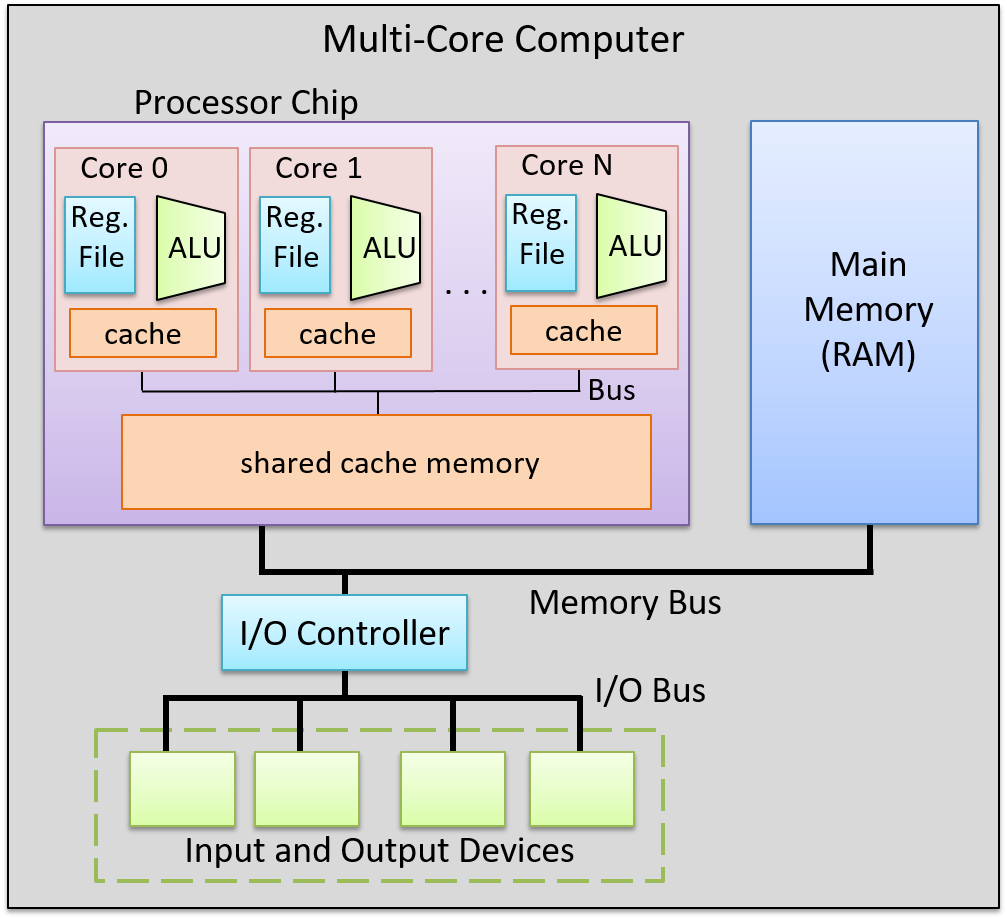
Control Processing Unit (CPU)
Processing Unit
The processing unit (PU) consists of three major subsections.
The first part is the arithmetic/logic unit (ALU), which performs mathematical and logical operations on integers. It takes the data operands sitting in registers and performs the operation based on the opcode from the instruction. It then produces an integer result, as well as a status flags, which encodes information about the result of the operation just performed (e.g. whether the integer result is negative (negative flag), zero (zero flag), if there is a carry-out bit from the operation (carry flag), or if there is integer overflow (overflow flag), etc.). These status flags are sometimes used by subsequent instructions that choose an action based on a particular condition.
Similarly, the second part of the PU is the floating-point unit (FPU), which performs arithmetic operations on floating-point values.
The fourth part of the PU is called the register file, which is the set of a small, fast unit of storage each called a register, used to hold program data and program instructions that are being executed by the ALU. These registers can each hold one data word.
Control Unit
The control unit (CU) drives the execution of program instructions by loading them from memory and feeding instruction operations and instruction operands through the processing unit. It also includes two special registers: the program counter (PC) keeps the memory address of the next instruction to execute, and the instruction register (IR) stores the instruction, loaded from memory, that is currently being executed.
Together, the control and processing units form the control processing unit (CPU), which is the part of the computer that executes program instructions on program data.
Timing Circuit
The CPU also contains a clock, which is a hardware crystal oscillator that generates a clock signal, which is a continuous stream of electrical pulses that coordinates all processor activity. Each pulse, known as a clock cycle, acts like a heartbeat, synchronizing when the ALU performs an operation, when registers capture or update values, and when data is transferred across buses. Without the clock signal, the PU’s components would have no reference for when to act. The clock speed (or clock rate) is the frequency of these cycles, measured in hertz (typically gigahertz).
Memory Unit
The memory unit stores both program instructions and program data, positioned close to the processing unit (PU) to reduce the time required for calculations. Its size varies depending on the system.
In modern computers, the memory unit is typically implemented as random access memory (RAM). In RAM, every storage location (address) can be accessed directly in constant time. Conceptually, RAM can be viewed as an array of addresses. Since the smallest addressable unit is one byte, each address corresponds to a single byte of memory. The address space spans from $0$ up to $2^{\text{natural data width}} - 1$, where the natural data width depends on the ISA.
Input and Output (I/O) Unit
The input unit consists of the set of devices that enable a user or program to get data from the outside world into the computer. The most common forms of input devices today are the keyboard and mouse. Cameras and microphones are other examples.
The output unit consists of the set of devices that relay results of computation from the computer back to the outside world or that store results outside internal memory. For example, the monitor and speakers are common output devices.
Some modern devices act both as an input and an output unit . For instance, touchscreen, act as both input and output, enabling users to both input and receive data from a single unified device. Solid-state drives and hard drives are another example of devices that act as both input and output devices, since they act as input devices when they store program executable files that the operating system loads into computer memory to run, and they act as output devices when they store files to which program results are written.
Buses
The communication channel compromised of a set of wires which as a whole connects the units so that they may transfer information in binary to another unit is called the bus. Typically, architectures have separate buses for sending different types of information between units:
- the data bus: transferring data between units
- the address bus: sending the memory address of a read or write request to the memory unit
- the control bus: send control (i.e., read/write/clock) signals notifying the receiving units to perform some action.
An important bus is the one which connects the CPU and the memory unit together. On 64-bit architectures, the data bus is made of 64 parallel wires, and therefore capable of 8-byte data transfers, where each wire can send 1 bit of information.
Instruction Set Architecture (ISA)
A particular CPU implements a specific instruction set architecture (ISA), which defines the set of instructions and their binary encoding, the set of CPU registers, the natural data width of a CPU, and the effects of executing instructions on the state of the processor. There are many different ISAs, notably MIPS, ARM, x86 (including x86-32 and x86-64). A microarchitecture defines the circuitry of an implementation of a specific ISA. Microarchitecture implementations of the same ISA can differ as long as they implement the ISA definition. For example, Intel and AMD produce different microprocessor implementations of x86-64.
Categories of ISAs
ISAs can be categorized based on two philosophies which describe how an ISA is structured and how instructions are meant to be implemented in hardware. These are the reduced instruction set computer (RISC), and complex instruction set computer (CISC).
Notable ISAs may be categorized as follows:
- CISC ISA: x86
- RISC ISAs: ARM, RISC-V, MIPS, IBM POWER
RISC ISAs have a small set of basic instructions that each execute within one clock cycle, and compilers combine sequences of several basic RISC instructions to implement higher-level functionality. It also supports simple addressing modes (i.e., ways to express the memory locations of program data), and fixed-length instructions.
In contrast, CISC ISAs have a large set of complex higher-level instructions that each execute in several cycles. It also supports more complicated addressing modes, and variable-length instructions.
CPU Performance
The following equation is commonly used to express a computer’s performance ability:
$$ \frac{\text{time}}{\text{program}} = \frac{\text{instructions}}{\text{program}} \times \frac{\text{cycles}}{\text{instruction}} \times \frac{\text{time}}{\text{cycle}} $$
CISC attempts to improve performance by minimizing the number of instructions per program (the first fraction), while RISC attempts to reduce the cycles per instruction (the second fraction), at the cost of the instructions per program.
Another way to measure performance is in terms of Instructions Per Cycle (IPC), which represents the average number of instructions the CPU can complete in one clock cycle, where a higher IPC indicates better CPU utilization and parallelism.
Instructions
Types of Instructions
- Data Transfer Instructions
- Arithmetic and logic Operations
- Arithmetic operations
- Bitwise operations
- Other math operations
- Control-flow instructions
- Conditional and unconditional
- Function calls and function returns
Memory Layout
At a high level, instructions are typically made of bits which encode:
- Opcode: specifies the operation (e.g.,
ADD,LOAD,STORE,BEQ, etc.). - Operands: indicate the data sources registers, immediates (constants encoded directly in the instruction), or memory addresses.
- Destination: indicates the destination register for storing the result of the operation
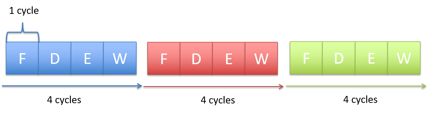
Instruction Cycle
Every single instruction follows a fetch-decode-execute cycle , which usually takes around 4 CPU cycles. This process starts with a program’s first instruction, and is repeated until the program exits.
Step 1: Fetch
- The CU retrieves the memory address stored in the PC, then places the address on the address bus and issues a read command over the control bus to request the instruction from memory.
- The MU reads the bytes at that address and transfers them back to the CU via the data bus.
- The CU stores these bytes in the IR.
- The CU increments the PC (typically by the size of the instruction), so it points to the next instruction in memory.
Step 2: Decode
- The CU interprets the instruction stored in the IR by decoding its bits according to the ISA’s instruction format, which involves identifying the opcode and the operand fields.
- If the instruction requires operands, the CU retrieves their values—whether from CPU registers, memory, or directly embedded in the instruction—and prepares them as inputs for the processing unit.
Step 3: Execute
- The CU sends control signals to components in the PU to carry out the instruction.
- The instruction is executed, potentially involving arithmetic operations, data movement, or other actions.
Step 4: Memory
- For store instructions: The CU writes data to memory by placing the target address on the address bus, a write command on the control bus, and the data value on the data bus. The MU receives these signals and writes the value to the specified memory location.
- For load instructions: The CU places the source address on the address bus and a read command on the control bus. The MU responds by placing the requested data on the data bus.
- For other instructions: This stage may be skipped if no memory access is required.
Step 5: Write-back
- The CU updates the CPU’s register file with the result of the executed instruction.
- If the instruction specified a destination register, the result is written back into that register, making it available for subsequent instructions.
Note
Not all instructions will need to go through all 5 stages.
Instruction-Level Parallelism
Pipelining
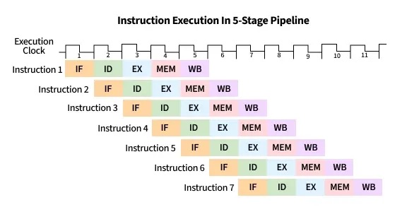
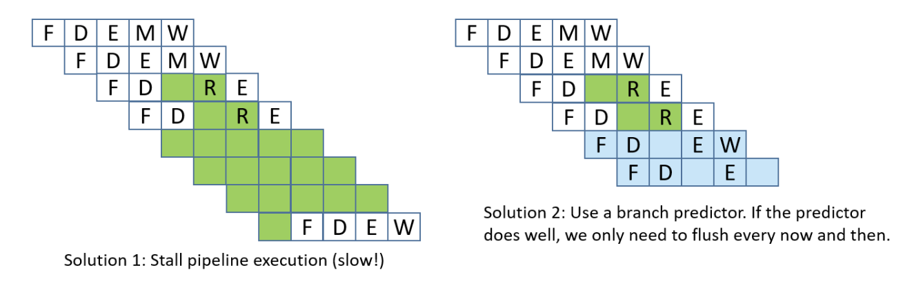
Notice that in the serial execution of the fetch-decode-execute cycle, the fetch hardware ends up being idle until the until the next instruction starts. This is wasteful! While instruction 1 is being decoded/executed/written back, the fetch unit could already be fetching instruction 2, 3, etc.
CPU pipelining is the idea of starting the execution of the next instruction before the current instruction has fully completed its execution. That is, pipelining will execute instructions in order, but it allows the execution of a sequence of instructions to overlap.
For example, in the first cycle, the first instruction enters the Fetch stage. In the second cycle, that instruction advances to Decode while the second instruction begins Fetch. In the third cycle, the first instruction reaches Execute, the second moves to Decode, and the third begins Fetch. In the fourth cycle, the first instruction enters the Memory stage, and the fourth instruction begins in the Fetch stage.
Finally, the first instruction enters in the write-back stage, and completes, where the second advances to the Memory stage, the third to Execute, and the fourth to Decode. At this point (i.e. after the fifth cycle), the pipeline is fully loaded, and so each stage of the CPU is busy with a different instruction, each one step behind the previous (which forms the staircase in the figure below). Once the pipeline is full, the CPU can complete one instruction every clock cycle, greatly improving instruction throughput. On the other hand, if each fetch-decode-execute cycle is performed sequentially, the instruction throughput would remain constant.
Hazards
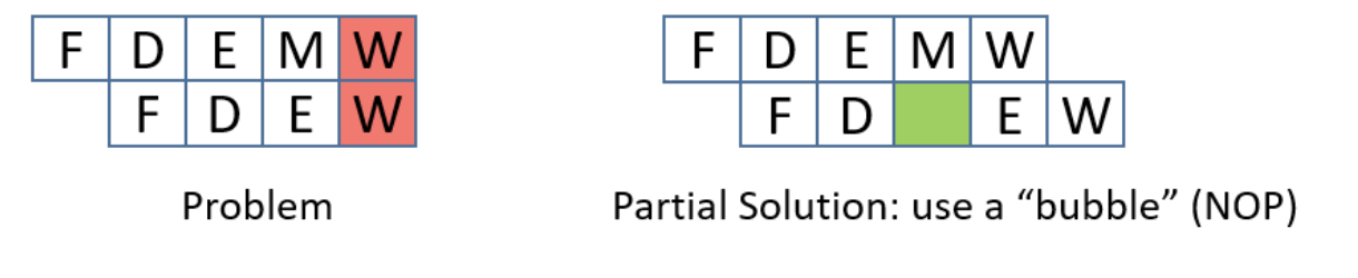
While pipelining improves instruction throughput by overlapping instruction stages, it can still suffer from hazards: a situation that prevents the next instruction in the pipeline from executing in its designated clock cycle. This causes the pipeline to stop or delay instruction advancement, which we call a pipeline stall. There are three particular hazards: data hazards, control hazards, and structural hazards. A data hazard is a hazard caused when an instruction depends on the result of a previous one that has not yet completed. A common solution involves inserting no operations (NOPs) (also called a pipeline bubbles) into the pipeline, notably the shorter instruction.
Consider the following instruction stream:
mov rax, qword ptr [0x84]   ; Load memory at 0x84 into RAX
add rax, 2                  ; Add 2 to RAX
The mov instruction (mov rax, qword ptr [0x84]) needs to read from memory (MEM stage) and then write the result to rax (WB stage), which takes five pipeline stages. The add instruction (add rax, 2) only needs four stages since it doesn’t go through the MEM stage. Because pipelining overlaps these stages, both instructions can be “in flight” at once — parts of both are being executed simultaneously.
However, since the mov instruction hasn’t finished writing to rax yet (it hasn’t reached its WB stage), the add instruction — which depends on the updated value in rax — reaches its EX stage early and tries to read rax before mov’s write-back is complete. This creates a read-after-write (RAW) hazard.
Also, since the mov takes five stages and the add takes four, their write-back stages line up so that both try to write to rax in the same cycle. This introduces another data hazard, a write-after-write (WAW) hazard.
To prevent this, the CPU can make all instructions effectively take five stages by inserting no operations (NOPs, or informally, pipeline bubbles).
NOPs delay the add until the mov has fully completed, preventing overlapping writes. However, inserting bubbles slows down the pipeline, since extra cycles are wasted waiting for results.
A more efficient solution is operand forwarding. Instead of stalling with NOPs, the CPU can forward the result of the mov instruction directly from the pipeline stage where it becomes available to the stage where the add needs it. This allows the add rax, 2 instruction to execute immediately once the loaded value is ready, without waiting for the mov to finish its write-back.
By using operand forwarding, the processor eliminates unnecessary bubbles, keeps the pipeline full, and executes both instructions efficiently.
A control hazard is a hazard when the pipeline doesn’t know which instruction to fetch next because it’s waiting for the outcome of a conditional branch instruction. This can cause the pipeline to make a wrong guess, requiring it to flush the incorrectly fetched instructions and restart, which slows down performance. To adress control hazards,many NOPs can be inserted by the compiler or assembler until the processor is sure that the branch is taken. Another solution involves eager execution, which execute both sides of the branch at the same time, and when the condition is finally known, it just chooses the right result. In x86, we see this through cmov. However, it brings some safety downsides, such as if one branch does something with side effects (like writing to memory or calling a function), you can’t execute it speculatively without changing program behavior, or if one branch dereferences a pointer that might be invalid, executing it early could cause a crash, and of course, inefficiency, as it also wastes work when one path’s results are thrown away. The most interesting solution is branch prediction, which involves a branch predictor, that predicts which way a branch will go, based on previous executions.
Lastly, structural hazards are hazards that arise when two instructions need the same hardware resource at the same time.
Out-of-Order Execution
The CPU can be further optimized by allowing out-of-order execution. This means instructions that are independent of one another can be executed in a different order than they appear in the program, as long as the final results respect program order.
For example, consider this instruction stream:
r3 = r1 * r2r4 = r2 + r3r7 = r5 * r6r8 = r1 + r7
There are two data hazards: instruction 2 depends on the result of instruction 1 (it needs the value of r3), and instruction 4 depends on the result of instruction 3 (it needs the value of r7). However, instructions 2 and 3 are independent of each other. Instead of stalling the pipeline while waiting for instruction 1 to finish, the CPU can begin executing instruction 3 in parallel, ensuring that hardware units stay busy.
Memory
Memory Hierarchy
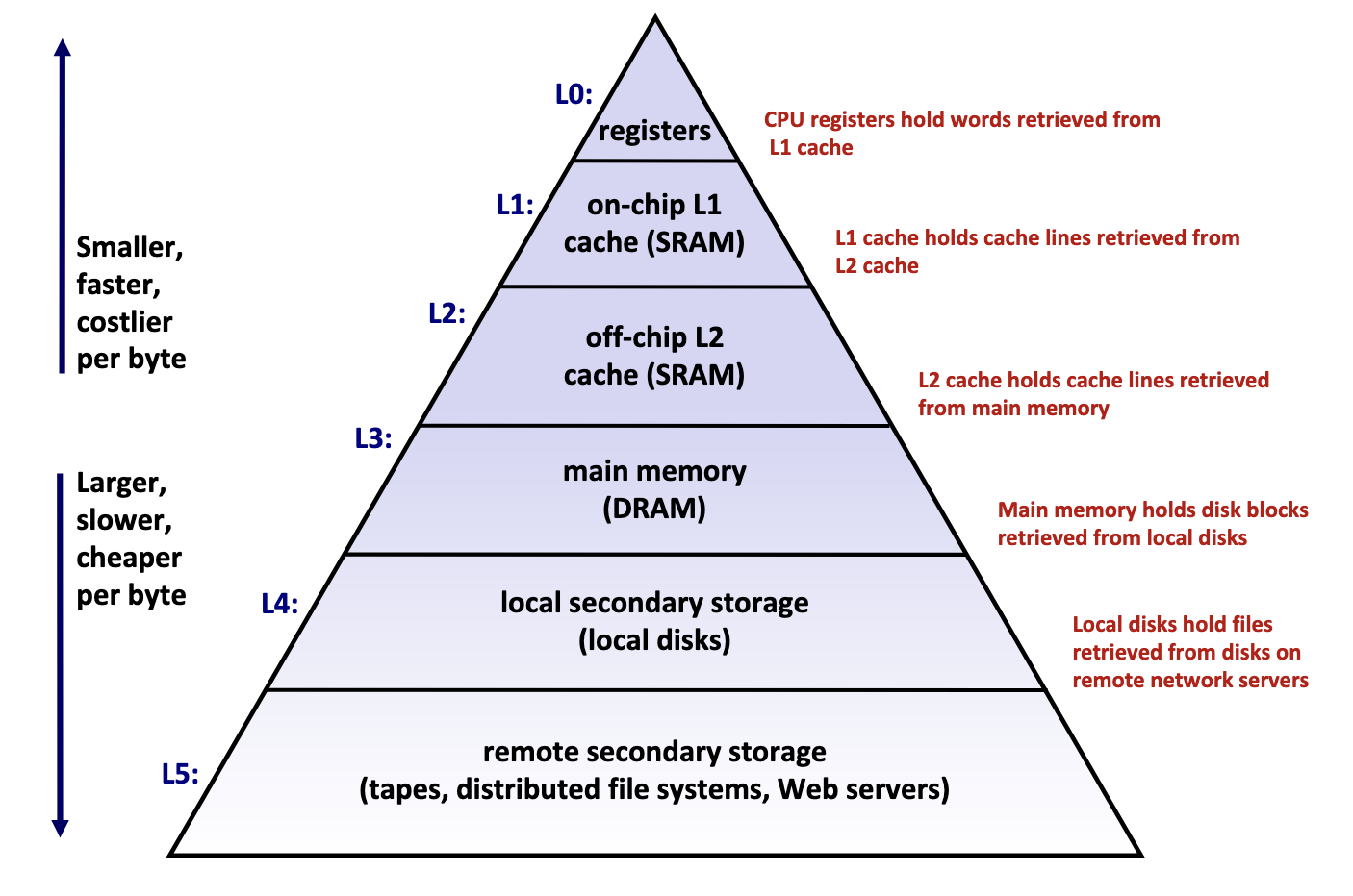
Memory hierarchy is typically divided into two broad categories:
- Primary storage: Devices the CPU can access directly using its instruction set, including registers, caches, and main memory. These devices are volatile, meaning they do not retain data when power is lost.
- Secondary storage: Devices that the CPU cannot access directly, requiring data to first be copied into primary storage before the CPU can operate on it. These devices are persistent or non-volatile, meaning they retain data when there are power outages.
Performance is evaluated primarily along three dimensions:
- Memory Latency: the time required for a device to deliver requested data after being instructed to do so, measured in time units (nanoseconds, milliseconds) or CPU cycles
- Memory Throughput: the amount of data that can be transferred between the device and main memory per unit time, typically measured in bytes per second.
- Memory Bandwidth: The upper bound on the amount of data that can be read per unit time, typically measured in bytes per second.
These two metrics are influenced by two key factors:
- The distance from the CPU plays a crucial role, as devices closer to the CPU’s processing units can deliver data more quickly.
- The underlying technology of the storage medium heavily influences performance. Registers and caches rely on extremely simple, compact circuits made of only a few logic gates, allowing signals to propagate almost instantly, while mechanical hard drives suffer from delays of 5-15 milliseconds due to the physical need to rotate and align read/write heads.
Takeaway: The faster the device, the smaller its storage capacity, and vice versa.
Primary Storage
Primary storage devices, notably CPU registers, CPU caches, and main memory, consist of random access memory (RAM), meaning the time required to access data remains constant regardless of the data’s location within the device.
Primary storage devices follows two main cell memory designs: Static RAM (SRAM), which stores data in small electrical circuits and represents the fastest type of memory used to build registers and caches, and Dynamic RAM (DRAM), which stores data using capacitors that hold electrical charges and must frequently refresh these charges to maintain stored values, making it ideal for implementing main memory.
Secondary Storage
The two most common secondary storage devices today are hard disk drives (HDDs) and flash-based solid-state drives (SSDs).
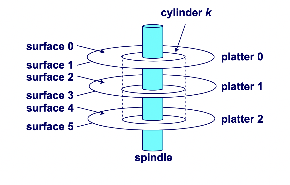
A hard drive consists of several flat, circular platters. Each platter has a upper surface and lower surface. Each surface is organized in concentric rings called tracks, and each track consists of sectors separated by gaps. Additionally, aligned tracks form a cylinder. In the centre of each platter, sits a spindle.
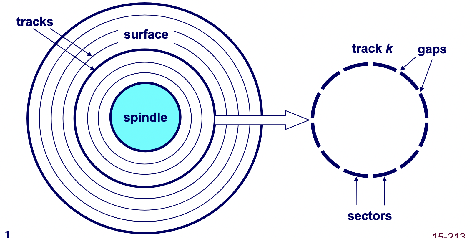
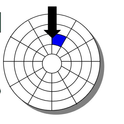
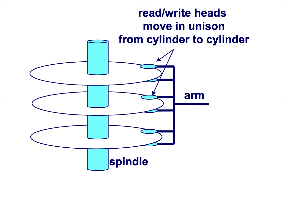
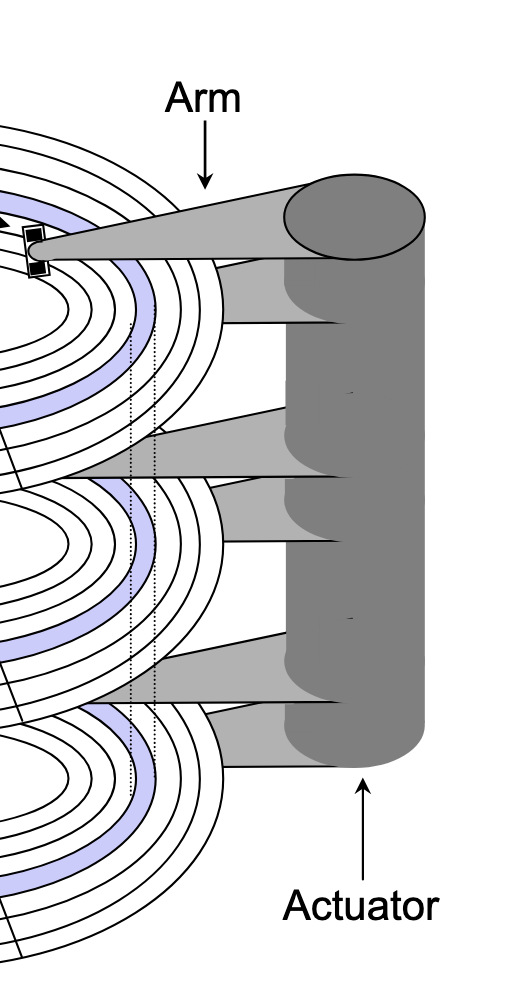
To read or write data, the mechanical arms, all attached to an actuator, where each arm with a read/write head at its tip, moves (i.e., extending or retracting) in unison across the platter to position the head over the cylinder containing the target sector (i.e., the sector holding the desired data). This step introduces a performance metric called seek time, where the typical average seek time is 3 to 5 ms. Then, the platters spins in counter-clockwise so that the target sector sits under the head. This step also introduces a performance metric called rotational latency, where the average rotational latency (in seconds) is found by $\frac{1}{2} \times \frac{1}{\text{RPM}} \times \frac{60 \text{ seconds}}{1 \text{ min}}$. Lastly, the data is read, where this step introduces a last performance metric called transfer time, calculated by $\frac{1}{\text{RPM}} \times \frac{1}{\text{average sectors per track}} \times \frac{60 \text{ seconds}}{1 \text{ min}}$
Locality of Reference
Locality of reference refers to the memory access pattern of a program where programs tend to use instructions and data with addresses near or equal to those they have used recently. There are two forms of locality: temporal locality, which refers to the pattern where a program is likely to access recently referenced items again in the near future, while spatial locality refers to the pattern where a program tend to access data that is nearby (in terms of memory address) to previously accessed data.
Caching
Background
To understand why caches are important, we have to understand the processor-memory bottleneck problem. According to Moore’s law, the number of transistors on microchips, and therefore processor performance, will double every two years. However, memory bus bandwidth improved much more slowly over the same period. This created a growing gap in improvement, where increasingly powerful processors were starved for data because they could request information faster than the memory system could deliver it. Caches are the solution which bridge this performance gap by.
A cache is computer memory with short access time built directly into your CPU used for storing copies of frequently or recently used instructions or data from main memory.
Mechanics
Cache Addressing
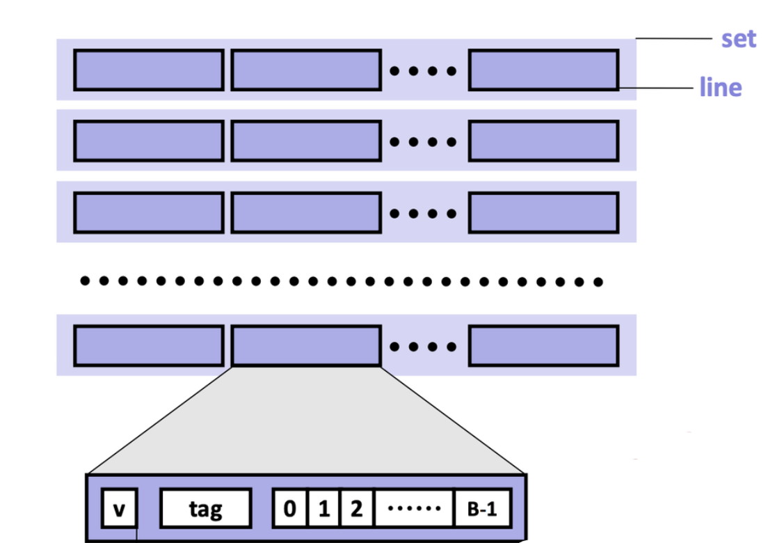
Cache is made of small chunks of memory copied from main memory, where a single chunk is called a cache line, typically capable of each storing 64 bytes. The cache can only load and store memory in multiples of a cache line (i.e., the data transfer unit is a cache line).
Each cache line consists of three sections: the valid bit, the tag, and the data block.
- Valid bit: Indicates whether the cache line contains valid, up-to-date data corresponding to some address in main memory.
- Tag: Stores the high-order bits of the memory address of the data currently cached.
- Data block: Contains the actual data copied from main memory.
Note
For caches employing the write-back write hit policy, then it also contains a dirtiness bit. The dirtiness bit is $1$when the cache line is dirty, and $0$ when it’s clean.
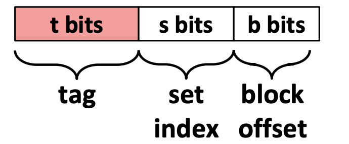
A cache memory address is split into three fields:
- Block offset: Tells which starting byte inside a data block the CPU wants. The number of bits $b$ allocated to the block offset field is $\log_2 (B)$, where $B$ is the data block size.
- Set index: Tells which set in the cache to look in. The number of bits $s$ allocated to the set index field is $\log_2 (S)$, where $S$ is the total sets.
- Tag: Tells which specific data block the CPU wants to access in the cache. The number of bits $t$ allocated to the tag field is $w - (s + b)$, where $w$ is word size.
Accessing the Cache
-
Locate the set
The cache uses the index bits from the memory address to identify which set in the cache might contain the desired block.
-
Check for a matching tag
The cache compares the tag bits from the memory address with the stored tag in each cache line of that set. If a match is found, and the cache line’s valid bit is set (i.e., the valid bit 1), we call this phenomenon a cache hit.
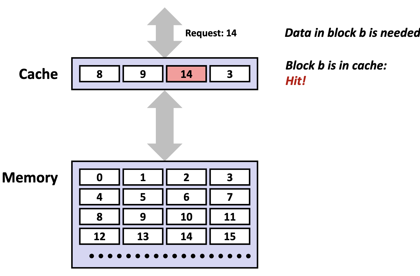
If no match is found, or the valid bit is 0, we call this unsucecssful access a cache miss.
There are three primary cases for a cache misses. A cold (compulsory) miss is a type of cache miss that happens when data is requested for the very first time, and therefore, is not yet present in the cache. A capacity miss is a type of cache miss that occurs when the cache is not large enough to hold all the data a program actively needs, called the working set, forcing existing data to be evicted to make room for new data. A conflict miss is a cache miss that occurs when a memory address maps to a cache location that is already occupied by a different cache line, despite the cache having free space elsewhere. The existing cache line is evicted and replaced with the cache line containing the requested memory address.
When a cache miss occurs, the cache controller first looks for an invalid cache line to store the requested data. If all cache lines are valid (i.e., their valid bits are set to 1), one cache line must be replaced. In set-associative and fully associative caches, a replacement policy (such as LRU) determines which line to evict. In a direct-mapped cache, however, each memory block maps to exactly one line, so that line is automatically selected. After selecting the cache line to be replaced, if the cache is a write-back cache, and the cache line is dirty, the cache will write back to the lower memory device. Then, the cache controller fetches the requested data block from the next lower level of memory, stores it in the selected line, and updates the line’s valid bit and tag. Finally, the specific bytes requested by the CPU are extracted from the cache line and delivered to the processor.
-
Perform the access (read or write)
On a read, the CPU retrieves the data directly from the cache line’s data block, beginning at the block offset from the memory address. On a write, the CPU updates the cache line’s data block, and may perform more actions depending on the cache write hit policy.
Issues
Although caches are designed to accelerate performance by keeping frequently used data close to the CPU, inefficient access patterns can cause the opposite effect.
Cache pollution occurs when the cache is filled with data that is unlikely to be reused soon, displacing more valuable data that would have benefited from being cached. This often happens in workloads with poor temporal locality.
Cache thrashing is the phenomenon where different memory addresses repeatedly map to the same cache lines, causing constant evictions and reloads. Thrashing leads to a high miss rate and can degrade performance to the point where the cache provides little or no benefit.
Cache Hierarchy
Modern processors organize caches into a three-tier hierarchy:
- L1 cache: the smallest and fastest cache, located directly on each CPU core for immediate access.
- L2 cache: larger and a bit slower than L1, usually dedicated to a single core but still very close to it.
- L3 cache: the largest and slowest of the three, typically shared among all cores on the processor to coordinate data efficiently.
| Level | Size |
|---|---|
| L1 | 32 KiB (each) |
| L2 | 256 KiB |
| L3 | 8000 KiB |
Instruction Cache and Data Cache
L1 caches are typically split into instruction caches (I-cache) and data caches (D-cache), following the Harvard Architecture design principle.
The primary advantage of separating instruction and data caches is eliminating contention between instruction fetches and data accesses. A CPU typically needs to fetch instructions every cycle to keep the pipeline fed, while simultaneously loading and storing data for instructions already in execution. With a unified cache, instruction fetches and data accesses occurring in the same cycle would compete for the same cache port — the read/write access path into the cache’s memory array. This competition creates a structural hazard, where multiple operations compete for the same hardware resource simultaneously, forcing the CPU to stall one operation until the resource becomes available. By splitting the L1 cache, instruction fetches and data accesses can occur simultaneously without interference. This parallelism keeps the pipeline busier and increases instructions per cycle (IPC), directly improving processor performance.
Separate caches also provide valuable design flexibility. Instruction streams exhibit predictable characteristics: they follow mostly sequential access patterns, are highly predictable, and are rarely self-modifying. In contrast, data accesses are more random and frequently involve writes. This behavioral difference allows hardware designers to optimize each cache type:
- I-cache optimization: Can be designed as read-only with sequential access patterns, enabling aggressive prefetching of subsequent instruction lines while avoiding the complexity and cost of write-back circuits, cache invalidation logic, and coherency protocols.
- D-cache optimization: Must handle the full complexity of read/write operations, cache coherency, and the unpredictable access patterns typical of data operations.
Cache Placement Policies
Cache placement policies are policies that determine where a particular memory address can be placed when it goes into a cache.
A fully-associative cache is a cache where a memory blocks are free to be stored anywhere in the cache. During each memory access, the system checks every cache line for the data in parallel, but it still remains a fairly expensive operation for reasonably-sized caches.
To address this inefficiency, caches impose restrictions on where specific memory blocks can reside. However, it does bring along a tradeoff. Since the cache is dramatically smaller than main memory, multiple memory addresses must inevitably map to the same cache locations — a phenomenon called cache aliasing. When two aliased addresses are frequently accessed and modified, they compete for the same cache line, creating what’s known as cache line contention.
A set-associative cache is a cache where a memory block maps to a specific set (i.e., a compartment of the cache), according to the index field encoded in the memory block’s address. Each of the sets contains $N$ cache lines, where we typically specify a cache as $N$-way set-associative. The cache hardware uses the index field of the requested memory address to select a set of the cache, then within that set, it will search all $N$ cache lines in parallel.
A direct-mapped cache maps each memory block to exactly one specific cache line based on the index field encoded in the memory block’s address. No searching is needed, as the hardware directly computes which single cache line to check.
As such, the total cache size (in bytes) is determined as follows:
$$ \text{cache size} = \text{total sets} \times \text{cache lines per set} \times \text{data block size} $$
Cache Write Policies
Cache reads do not involve upholding consistency with main memory. However, for cache writes, the CPU must decide how to handle updates to the underlying main memory.
Write Hit Policies
- Write-through: The cache immediately propagates all writes to the lower memory whenever the cache has been written to, to ensure that memory across different volatile storage devices remain synchronized at all times.
- Write-back: The cache defers writes to the lower memory until absolutely necessary. Cache lines that have been modified but not yet written to the lower memory are considered dirty, where they’ll need to eventually write its contents to lower memory (whether that’s before an eviction, or an explicit flush).
Write Miss Policies
- Write-allocate (fetch-on-write): The cache first loads the entire block from main memory into the cache, and then performs the write in the cache. This policy is typically paired with the write-back cache hit policy, because once the block is loaded, multiple writes can be performed locally without repeatedly accessing main memory.
- No-write-allocate (write-around): The data is written directly to main memory, and the cache is not updated or allocated for that address. This policy is often paired with the write-through cache hit policy, since write-through already ensures main memory is always updated; combining it with write-allocate would unnecessarily duplicate work and waste time.
Handles
Background
Handles are particular bit fields used as indirection, similar to tagged pointers.
They have notable benefits over raw pointers:
- Stable: Handles remains valid even if the underlying resource can be moved, swapped, or reallocated, while a pointer would be invalidated in the same scenario.
- Compact Representation: Handles can be smaller than native pointers. Notably, if you know your memory pool is less than 4 GiB, a
u32handle is enough, thereby saving memory. - Can Cross Abstraction Boundaries: Pointers are tied to one process, and therefore, one address space. Handles can be shared across threads, modules, or even across processes. The receiver only needs to know the handle format, not the actual memory layout.
- Control: On top of storing the index, handles can also encode metadata (e.g., generation counter, the underlying array within an SoA, etc.).
Implementation
Below is a compact, generation-checked handle table. Each handle packs the slot index and a generation counter into a u32, allowing stale handles to be rejected when a slot is reused.
#![allow(unused)]
fn main() {
/// Packs a 24-bit index and an 8-bit generation counter into a u32.
#[derive(Copy, Clone, Debug, PartialEq, Eq, Hash)]
struct Handle(u32);

impl Handle {
    fn new(index: u32, generation: u8) -> Self {
        debug_assert!(index < (1 << 24));
        Self((generation as u32) << 24 | index)
    }

    fn index(self) -> usize {
        (self.0 & 0x00FF_FFFF) as usize
    }

    fn generation(self) -> u8 {
        (self.0 >> 24) as u8
    }
}

/// Stores values in slots addressed by handles; rejects stale handles via generation checks.
struct HandleTable<T> {
    slots: Vec<Slot<T>>,
    free_list: Vec<usize>,
}

struct Slot<T> {
    generation: u8,
    value: Option<T>,
}

impl<T> HandleTable<T> {
    fn new() -> Self {
        Self {
            slots: Vec::new(),
            free_list: Vec::new(),
        }
    }

    fn insert(&mut self, value: T) -> Handle {
        if let Some(index) = self.free_list.pop() {
            let slot = &mut self.slots[index];
            slot.generation = slot.generation.wrapping_add(1);
            slot.value = Some(value);
            return Handle::new(index as u32, slot.generation);
        }

        let index = self.slots.len();
        assert!(index < (1 << 24), "Handle index overflow");
        self.slots.push(Slot {
            generation: 0,
            value: Some(value),
        });
        Handle::new(index as u32, 0)
    }

    fn get(&self, handle: Handle) -> Option<&T> {
        let index = handle.index();
        let slot = self.slots.get(index)?;
        (slot.generation == handle.generation()).then(|| slot.value.as_ref()).flatten()
    }

    fn get_mut(&mut self, handle: Handle) -> Option<&mut T> {
        let index = handle.index();
        let slot = self.slots.get_mut(index)?;
        (slot.generation == handle.generation()).then(|| slot.value.as_mut()).flatten()
    }

    fn remove(&mut self, handle: Handle) -> Option<T> {
        let index = handle.index();
        let slot = self.slots.get_mut(index)?;
        if slot.generation != handle.generation() {
            return None;
        }
        let value = slot.value.take()?;
        self.free_list.push(index);
        Some(value)
    }
}
}
Struct of Arrays
Background
Struct of Arrays (SoA) is a data layout where you store each field in its own contiguous array (can be as the struct’s field, a global variable, or a local variable), which provides:
- Low memory usage (there’s only padding for array fields, while in a AoS layout, there’s padding for every element in the array)
- Good memory bandwidth utilization for batched code (i.e. if you have a loop that process several objects that only accesses a few of the fields, then the SoA layout reduces the amount of data that needs to be loaded).
#![allow(unused)]
fn main() {
struct MySoA {
    field1: Vec<Type1>,
    field2: Vec<Type2>,
    // ...
    fieldN: Vec<TypeN>,
}
}
It’s inverse is the more common data layout, called Array of Structs (AoS).
Example
To achieve polymorphism, we can use the SoA and/or the AoS layout.
AoS with Enum-based Polymorphism
#![allow(unused)]
fn main() {
struct Shape {
    x: f32,
    y: f32,
    kind: ShapeKind,
}

enum ShapeKind {
    Circle { radius: f32 },
    Rectangle { width: f32, height: f32 },
    Triangle { base: f32, height: f32 },
}
}
AoS with Subclass-based (via Composition) Polymorphism
#![allow(unused)]
fn main() {
struct Shape {
    tag: Tag,
    x: f32,
    y: f32,
}

enum Tag {
    Circle,
    Rectangle,
    Triangle,
}

struct Circle {
    base: Shape,
    radius: f32,
}

struct Rectangle {
    base: Shape,
    width: f32,
    height: f32,
}

struct Triangle {
    base: Shape,
    base_len: f32,
    height: f32,
}
}
Hybrid AoS and SoA Variant-Encoding-based Polymorphism
#![allow(unused)]
fn main() {
struct Shape {
    tag: Tag,
    x: f32,
    y: f32,
    extra_payload_idx: u32,
}

enum Tag {
    Circle,
    Rectangle,
    Triangle,
}

struct CirclePayload {
    radius: f32,
}
struct RectanglePayload {
    width: f32,
    height: f32,
}
struct TrianglePayload {
    base: f32,
    height: f32,
}

// Layout at runtime:
//  - One Vec<Shape>
//  - Additional Vec<CirclePayload>, Vec<RectanglePayload>, and/or Vec<TrianglePayload>
//    indexed by Shape.extra_payload_idx as required

// Example of accessing the extra data:
match shapes[i].tag {
    Tag::Circle      => circle_payloads[shapes[i].extra_payload_idx].radius,
    Tag::Rectangle   => rectangle_payloads[shapes[i].extra_payload_idx],
    Tag::Triangle    => triangle_payloads[shapes[i].extra_payload_idx],
}
}
Struct Packing
Background
Alignment refers to the set of valid starting addresses for objects of a given type. A type’s natural alignment is the default alignment, determined by the platform, that enables efficient memory access (i.e. single-instruction loads & stores). Without natural alignment, a value might be placed such that it straddles machine-word boundaries. As a result, the CPU may need to perform multiple memory accesses and combine the pieces in registers, which increases the cost of reading or writing the value. In Rust, you can check a type’s alignment using std::mem::align_of.
For composite data types, notably structs or unions, the compiler often inserts extra unused bytes, called padding, to ensure each field begins at an address satisfying its own alignment and/or the alignment of the entire data structure. The compiler inserts internal padding before a field whenever the current struct offset isn’t aligned to the natural alignment requirement of the next field (i.e., $(\text{current offset} \mod \text{field alignment}) \neq 0$). The compiler also inserts trailing padding at the end to satisfy overall alignment requirements.
The data structure size is the total number of bytes the data structure occupies in memory, including both actual data and any inserted padding. You can retrieve this size using std::mem::size_of.
We also say a type is self-aligned to describe that its alignment equals its size.
The following table lists common types along with their natural alignment and size (in bytes) on a x86-64 system:
| Type | Natural Alignment (bytes) | Size (bytes) |
|---|---|---|
| Primitive | Same as size | bool = 1, u8 / i8 = 1, u16 / i16 = 2, char = 4, f32 / i32 / u32 = 4, f64 / i64 / u64 = 8, u128 / i128 = 16, usize / isize = 8 |
| Array / Slice | According to its element’s natural alignment | $\text{element size} \times \text{number of elements}$ |
| Pointer | 8 | 8 |
| Structure | Largest natural alignment among its fields | $\text{field sizes} + \text{internal padding} + \text{trailing padding}$ |
Note
In C, the order of fields of a struct is preserved exactly as written, while in Rust, the compiler may reorder fields to reduce padding unless you use the
#[repr(C)]attribute.
Field Re-Ordering
A common technique to pack a struct is re-ordering fields by decreasing natural alignment, since a field with larger alignment guarantees that any following smaller-alignment field will already be properly aligned:
#![allow(unused)]
fn main() {
#[repr(C)]
struct DefaultStruct {
    c: u8,        // 1 byte
                  // 7 bytes of field padding
    p: *const u8, // 8 bytes
    x: i16,       // 2 bytes
                  // 6 bytes of trailing padding
}
                  // total size: 24 bytes
}
#![allow(unused)]
fn main() {
#[repr(C)]
struct PackedStruct {
p: *const u8, // 8 bytes
x: i16, // 2 bytes
c: u8, // 1 byte
// 5 bytes of trailing padding
}
// total size: 16 bytes
}Another common trick is to group fields of the same alignment and same size together (on top of applying the trick above):
#![allow(unused)]
fn main() {
#[repr(C)]
struct DefaultStruct {
    a: i32,   // 4 bytes
    c1: u8,   // 1 byte
              // 3 bytes of field padding
    b: i32,   // 4 bytes
    c2: u8,   // 1 byte
              // 1 byte of field padding
    s1: i16,  // 2 bytes
    s2: i16,  // 2 bytes
              // 2 bytes of trailing padding
}
              // total size: 20 bytes
}
#![allow(unused)]
fn main() {
#[repr(C)]
struct PackedStruct {
a: i32, // 4 bytes
b: i32, // 4 bytes
s1: i16, // 2 bytes
s2: i16, // 2 bytes
c1: u8, // 1 byte
c2: u8, // 1 byte
// 2 bytes of trailing padding
}
// total size: 16 bytes
}Compiler Struct Packing
In Rust, you can add an attribute to force the compiler to lay out struct fields back-to-back with no padding, thereby breaking natural alignment:
#![allow(unused)]
fn main() {
#[repr(packed)]
struct PackedStruct {
    a: u8,
    b: i32,
    c: f64,
}
}
Note
Accessing unaligned fields in packed structs may lead to significantly slower code or even cause undefined behaviour on some platforms which can’t handle unaligned access at all. However, others, notably Daniel Lemire, argue to not worry about alignment.
Bit Packing
Bit Fields
Bit fields refers to the technique of subdividing an integer into multiple consecutive bit ranges, with each range functioning as an individual data field. This technique treats the integer as a compact storage container, where the arrangement and size of each field must be defined in advance.
#![allow(unused)]
fn main() {
pub struct BitField(u32);

#[derive(Debug, PartialEq, Clone, Copy)]
pub enum FieldId {
    Field1,
    Field2,
    Field3,
    Field4,
    Field5,
}

#[derive(Debug, PartialEq)]
pub enum BitFieldError {
    InvalidField,
    ValueTooLarge(u32),
}

impl BitField {
    // Overall visualization:
    // | 31 30 29 28 | 27 ... 18      | 17 ... 12  | 11 10 9 8 | 7 ... 0  |
    // +-------------+----------------+------------+-----------+----------+
    // |  Field5     |   Field4       |  Field3    |  Field2   | Field1   |
    // |   4 bits    |  10 bits       |  6 bits    |  4 bits   | 8 bits   |

    // bits 0 to 7, possible values from 0 to 255
    const FIELD1_START: u32 = 0;
    const FIELD1_WIDTH: u32 = 8;

    // bits 8 to 11, possible values from 0 to 15
    const FIELD2_START: u32 = 8;
    const FIELD2_WIDTH: u32 = 4;

    // bits 12 to 17, possible values from 0 to 63
    const FIELD3_START: u32 = 12;
    const FIELD3_WIDTH: u32 = 6;

    // bits 18 to 27, possible values from 0 to 1023
    const FIELD4_START: u32 = 18;
    const FIELD4_WIDTH: u32 = 10;

    // bits 28 to 31, possible values from 0 to 15
    const FIELD5_START: u32 = 28;
    const FIELD5_WIDTH: u32 = 4;

    pub const fn new() -> Self {
        Self(0)
    }

    pub fn set_field(&mut self, field: FieldId, value: u32) -> Result<(), BitFieldError> {
        let (start, width) = Self::get_field_info(field);
        let max_value = Self::get_max_value(width);
        if value > max_value {
            return Err(BitFieldError::ValueTooLarge(value));
        }
        let mask = Self::get_field_mask(start, width);
        self.0 = (self.0 & !mask) | ((value << start) & mask);
        Ok(())
    }

    pub fn get_field(&self, field: FieldId) -> u32 {
        let (start, width) = Self::get_field_info(field);
        let mask = Self::get_field_mask(start, width);
        (self.0 & mask) >> start
    }

    pub fn clear_field(&mut self, field: FieldId) -> Result<(), BitFieldError> {
        self.set_field(field, 0)
    }

    fn get_field_info(field: FieldId) -> (u32, u32) {
        match field {
            FieldId::Field1 => (Self::FIELD1_START, Self::FIELD1_WIDTH),
            FieldId::Field2 => (Self::FIELD2_START, Self::FIELD2_WIDTH),
            FieldId::Field3 => (Self::FIELD3_START, Self::FIELD3_WIDTH),
            FieldId::Field4 => (Self::FIELD4_START, Self::FIELD4_WIDTH),
            FieldId::Field5 => (Self::FIELD5_START, Self::FIELD5_WIDTH),
        }
    }

    fn get_field_mask(start: u32, width: u32) -> u32 {
        ((1u32 << width) - 1) << start
    }

    fn get_max_value(width: u32) -> u32 {
        (1u32 << width) - 1
    }
}
}
Bit Flags
Bit flags refers to the technique of treating individual bits within an integer as separate boolean toggles, where each bit indicates whether a specific condition, or option is active or inactive. The number of flags is typically predetermined and usually occupies only a portion of the integer’s available bits.
#![allow(unused)]
fn main() {
pub struct BitFlags(u8);

#[derive(Debug, PartialEq)]
pub enum BitFlagsError {
    InvalidFlag(u8),
}

impl BitFlags {
    pub const FLAG1: u8 = 0x01;
    pub const FLAG2: u8 = 0x02;
    pub const FLAG3: u8 = 0x04;
    pub const FLAG4: u8 = 0x08;

    const VALID_FLAGS: u8 = Self::FLAG1 | Self::FLAG2 | Self::FLAG3 | Self::FLAG4;

    pub const fn new() -> Self {
        Self(0)
    }

    pub fn set(&mut self, flags: u8) -> Result<(), BitFlagsError> {
        if (Self::VALID_FLAGS & flags) != flags {
            return Err(BitFlagsError::InvalidFlag(!Self::VALID_FLAGS & flags));
        }
        self.0 |= flags;
        Ok(())
    }

    pub fn clear(&mut self, flags: u8) -> Result<(), BitFlagsError> {
        if (Self::VALID_FLAGS & flags) != flags {
            return Err(BitFlagsError::InvalidFlag(!Self::VALID_FLAGS & flags));
        }
        self.0 &= !flags;
        Ok(())
    }

    pub fn toggle(&mut self, flags: u8) -> Result<(), BitFlagsError> {
        if (Self::VALID_FLAGS & flags) != flags {
            return Err(BitFlagsError::InvalidFlag(!Self::VALID_FLAGS & flags));
        }
        self.0 ^= flags;
        Ok(())
    }

    pub fn contains_any(&self, flags: u8) -> Result<bool, BitFlagsError> {
        if (Self::VALID_FLAGS & flags) != flags {
            return Err(BitFlagsError::InvalidFlag(!Self::VALID_FLAGS & flags));
        }
        Ok((self.0 & flags) != 0)
    }
}
}
SIMD
Background
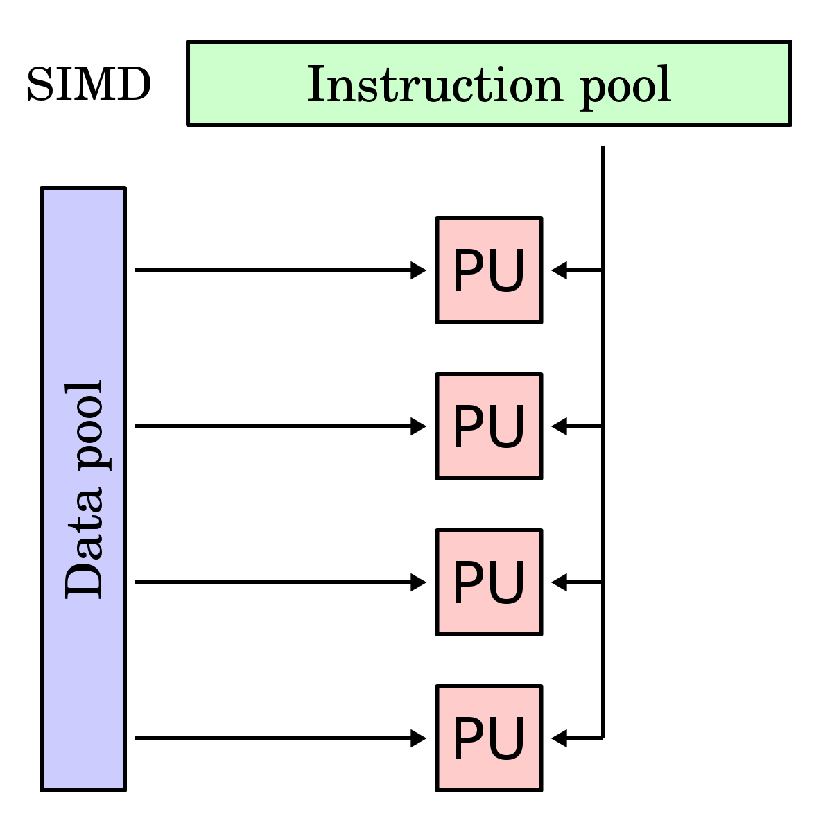
Single Instruction, Multiple Data (SIMD) is a form of data parallelism in which one instruction operates on multiple values simultaneously. This is achieved using vector registers, which hold multiple elements at once. Each slot within a vector register is called a lane, and operations on vector registers are called vector operations. On the other hand, scalar operations act on a single value at a time.
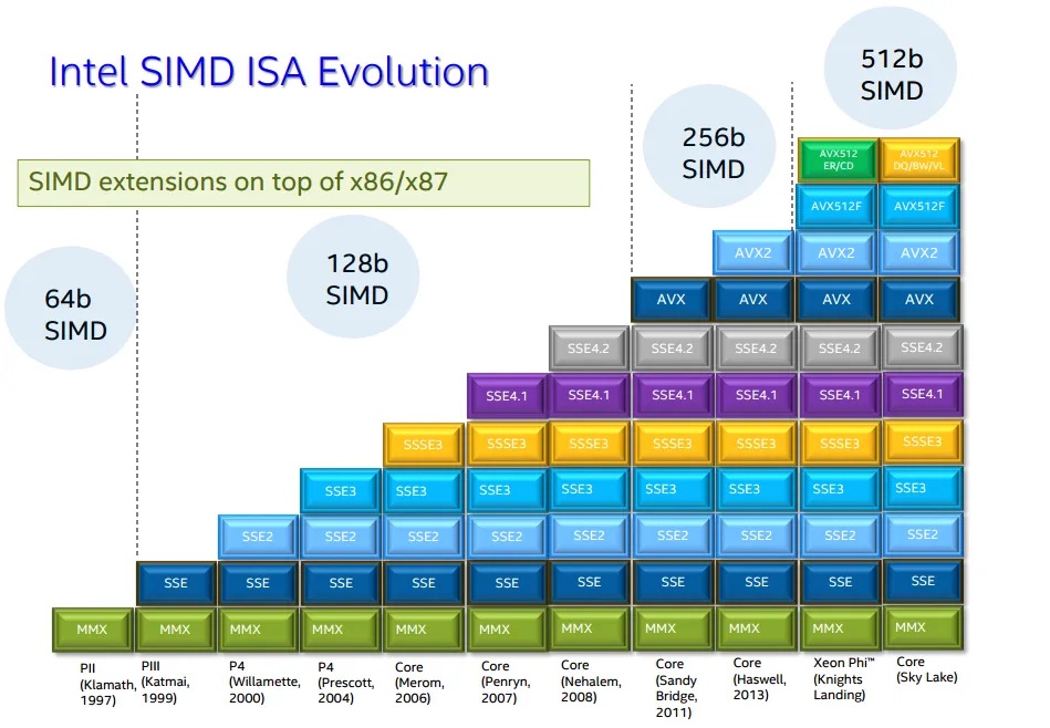
SIMD instruction set extensions are optional CPU features that add vector operations using vector registers. The instruction set architecture defines which SIMD instruction set extensions are possible, but it is up to the specific processor implementation to decide which of those extensions to support, and which vector widths of the chosen SIMD extension it will implement.
| ISA | SIMD Instruction Set Extension | First-Class Native Vector Widths |
|---|---|---|
| x86-64 | SSE, SSE2, SSE3, SSE4.1, SSE4.2 | 128 bits (fixed) |
| x86-64 | AVX | 256 bits (fixed, float only) |
| x86-64 | AVX2 | 256 bits (fixed, int + float) |
| x86-64 | AVX-512 | 512 bits (fixed) |
| AArch64 | NEON | 64 bits (fixed), 128 bits (fixed) |
| AArch64 | SVE | 128–2048 bits (scalable in 128-bit increments) |
| AArch64 | SVE2 | 128–2048 bits (scalable in 128-bit increments, more types) |
Note
Each generation of x86-64 SIMD extensions builds upon the previous one. When using narrower vector operations from older instruction sets, they operate on the lower portion of the wider registers introduced in newer extensions.
Note
To check what SIMD instruction set extensions your CPU supports, run
lscpu, and look at theFlagsoutput.
Rust API
Portable SIMD
Warning
Portable SIMD in Rust requires the Rust nightly compiler. To install it, run
rustup toolchain install nightly, then temporarily set it to the default compiler viarustup default nightly
Vendor SIMD Intrinsics
std::arch module and Intel Intrinsics Guide
Note
When writing non-portable SIMD code, consider using Dynamic CPU Feature Detection since this approach allows:
- The same binary to work on all CPUs
- Automatic use of the fastest available instructions
- Users don’t need to worry about compatibility issues
You can also use static CPU feature detection (via
RUSTFLAGS), which bakes specific SIMD instruction set extensions into the entire binary, but is discouraged as this will crash on CPUs that don’t support those features.
Example
Description
Given a slice of bytes haystack and a byte needle, find the first occurrence of needle in haystack.
Solution
#![allow(unused)]
#![feature(portable_simd)]
fn main() {
use std::simd::cmp::SimdPartialEq;
use std::simd::u8x32;

pub fn find(haystack: &[u8], needle: u8) -> Option<usize> {
    const VECTOR_WIDTH: usize = 32;

    // For short strings (less than 16 bytes), use simple iteration instead of SIMD
    if haystack.len() < VECTOR_WIDTH {
        return haystack.iter().position(|&b| b == needle);
    }

    // Perform SIMD on strings of at least 32 bytes.
    //
    // For every 32-byte chunk of the haystack, we create two SIMD vectors: one for the 16-byte
    // chunk of the haystack we're working on, `haystack_vec`, and one 16-byte SIMD vector containing
    // 16-bytes of just `needle`, `needle_vec` such that we can compare each byte against the needle in parallel using `simd_eq`,
    // producing a mask.
    //
    // This SIMD mask is a vector of booleans, like:
    //   [false, false, false, true, false, ...]
    //
    // We convert this mask into a compact bitmask with `to_bitmask()`, which gives us
    // a u32 where each bit corresponds to an entry in the SIMD mask:
    //
    //   - A `true` in the SIMD mask becomes a `1` in the bitmask.
    //   - A `false` becomes a `0`.
    //
    // Importantly: the first element of the mask (index 0) maps to the least significant bit (bit 0)
    // in the bitmask, mask[1] maps to bit 1, and so on. This means `bitmask.trailing_zeros()`
    // directly gives us the index of the first `true` in the mask.
    //
    // So if the bitmask is, say, 0b00001000, then the first match was at index 3.
    //
    // Using `bitmask.trailing_zeros()` gives us the index of the first `true` in the mask.
    // We then add the chunk offset to get the actual index in the full haystack.
    let needle_vec = u8x32::splat(needle);

    let mut offset = 0;
    while offset + VECTOR_WIDTH <= haystack.len() {
        let chunk = &haystack[offset..offset + VECTOR_WIDTH];
        let haystack_vec = u8x32::from_slice(chunk);
        let mask = haystack_vec.simd_eq(needle_vec);
        let bitmask = mask.to_bitmask();

        if bitmask != 0 {
            return Some(offset + bitmask.trailing_zeros() as usize);
        }
        offset += VECTOR_WIDTH;
    }

    // Handle remaining bytes (less than 32) that couldn't be processed with SIMD
    haystack[offset..]
        .iter()
        .position(|&b| b == needle)
        .map(|pos| offset + pos)
}
}