Microarchitecture
von Neumann architecture
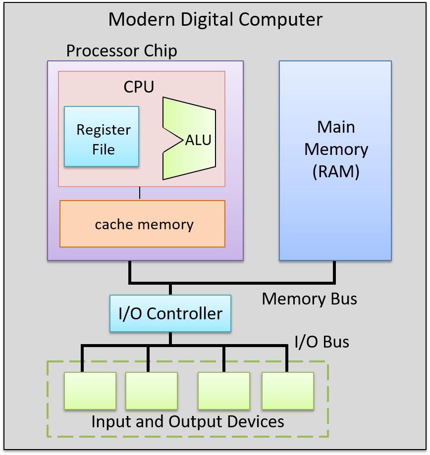
Control Processing Unit (CPU)
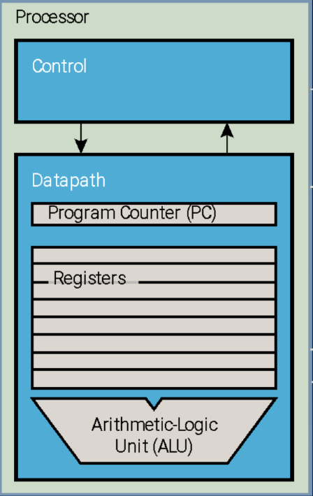
Datapath Unit
The datapath unit is the portion of the processor that contains the hardware necessary to perform operations required by the processor.
It contains a few components:
- Arithmetic/logic unit (ALU): performs mathematical and logical operations on integers. It takes the data operands sitting in registers and performs the operation based on the opcode from the instruction. It then produces an integer result, as well as a status flags, which encodes information about the result of the operation just performed (e.g. whether the integer result is negative (negative flag), zero (zero flag), if there is a carry-out bit from the operation (carry flag), or if there is integer overflow (overflow flag), etc.). These status flags are sometimes used by subsequent instructions that choose an action based on a particular condition.
- Floating-point units (FPUs): similar as the ALU, but performs arithmetic operations on floating-point values.
- Register file: set of a small, fast unit of storage each called a register, used to hold program data and program instructions that are being executed by the ALU. These registers can each hold one data word.
- Program counter (PC): a special register used to store the memory address of the next instruction to execute.
Control Unit
The control unit (CU) is the portion of the processor that tells the datapath what needs to be done. It describes the signals needed to ensure the elements of the datapath correctly execute an instruction.
Some of its notable components:
- Instruction register (IR): holds the current instruction being executed.
- Instruction decoder: decodes the instruction in the instruction register, and generates the appropriate control signals.
The clock is a separate physical component (a crystal oscillator) feeding into the entire CPU, which generates a clock signal: a continuous stream of electrical pulses that coordinates all processor activity. Each pulse, known as a clock cycle, acts like a heartbeat, synchronizing when the ALU performs an operation, when registers capture or update values, and when data is transferred across buses. Without the clock signal, the datapath's components would have no reference for when to act. The clock speed (or clock rate) is the frequency of these cycles, measured in hertz (typically gigahertz).
Memory Unit
The memory unit stores both program instructions and program data, positioned close to the processing unit (PU) to reduce the time required for calculations. Its size varies depending on the system.
In modern computers, the memory unit is typically implemented as random access memory (RAM). In RAM, every storage location (address) can be accessed directly in constant time. Conceptually, RAM can be viewed as an array of addresses. Since the smallest addressable unit is one byte, each address corresponds to a single byte of memory. The address space spans from 0 up to 2^{\text{word}} - 1, where the word depends on the ISA.
Input and Output (I/O) Unit
The input unit consists of the set of devices that enable a user or program to get data from the outside world into the computer. The most common forms of input devices today are the keyboard and mouse. Cameras and microphones are other examples.
The output unit consists of the set of devices that relay results of computation from the computer back to the outside world or that store results outside internal memory. For example, the monitor and speakers are common output devices.
Some modern devices act both as an input and an output unit. For instance, touchscreen, act as both input and output, enabling users to both input and receive data from a single unified device. Solid-state drives and hard drives are another example of devices that act as both input and output devices, since they act as input devices when they store program executable files that the operating system loads into computer memory to run, and they act as output devices when they store files to which program results are written.
Buses
The communication channel comprised of a set of wires which as a whole connects the units so that they may transfer information in binary to another unit is called the bus. Typically, architectures have separate buses for sending different types of information between units:
- the data bus: transferring data between units
- the address bus: sending the memory address of a read or write request to the memory unit
- the control bus: send control (i.e., read/write/clock) signals notifying the receiving units to perform some action.
An important bus is the one which connects the CPU and the memory unit together. On 64-bit architectures, the data bus is made of 64 parallel wires, and therefore capable of 8-byte data transfers, where each wire can send 1 bit of information.
Instruction Set Architecture (ISA)
A particular CPU implements a specific instruction set architecture (ISA), which defines the set of instructions and their binary encoding, the set of CPU registers, the natural data width of a CPU, and the effects of executing instructions on the state of the processor. There are many different ISAs, notably MIPS, ARM, x86 (including x86-32 and x86-64). A microarchitecture defines the circuitry of an implementation of a specific ISA. Microarchitecture implementations of the same ISA can differ as long as they implement the ISA definition. For example, Intel and AMD produce different microprocessor implementations of x86-64.
Categories of ISAs
ISAs can be categorized based on two philosophies which describe how an ISA is structured and how instructions are meant to be implemented in hardware. These are the reduced instruction set computer (RISC), and complex instruction set computer (CISC).
Notable ISAs may be categorized as follows:
- CISC ISA: x86
- RISC ISAs: ARM, RISC-V, MIPS, IBM POWER
RISC ISAs have a small set of basic instructions that each execute within one clock cycle, and compilers combine sequences of several basic RISC instructions to implement higher-level functionality. It also supports simple addressing modes (i.e., ways to express the memory locations of program data), and fixed-length instructions.
In contrast, CISC ISAs have a large set of complex higher-level instructions that each execute in several cycles. It also supports more complicated addressing modes, and variable-length instructions.
CPU Performance
The following equation is commonly used to express a computer's performance ability:
\frac{\text{time}}{\text{program}} = \frac{\text{instructions}}{\text{program}} \times \frac{\text{cycles}}{\text{instruction}} \times \frac{\text{time}}{\text{cycle}}
CISC attempts to improve performance by minimizing the number of instructions per program (the first fraction), while RISC attempts to reduce the cycles per instruction (the second fraction), at the cost of the instructions per program.
Another way to measure performance is in terms of Instructions Per Cycle (IPC), which represents the average number of instructions the CPU can complete in one clock cycle, where a higher IPC indicates better CPU utilization and parallelism.
Instructions
Types of Instructions
- Data Transfer Instructions
- Arithmetic and logic Operations
- Arithmetic operations
- Bitwise operations
- Other math operations
- Control-flow instructions
- Conditional and unconditional
- Function calls and function returns
Memory Layout
At a high level, instructions are typically made of bits which encode:
- Opcode: specifies the operation (e.g.,
ADD,LOAD,STORE,BEQ, etc.). - Operands: indicate the data sources: registers, immediates (constants encoded directly in the instruction), or memory addresses.
- Destination: indicates the destination register for storing the result of the operation (note: not all instructions have one, e.g.,
STORE,CMP,BEQ). - Addressing Mode: specifies how to interpret the operand (i.e., how to find the actual data). Common modes:
- Immediate: the operand is the data (e.g.,
ADD R1, #5, where 5 is the value itself) - Register: the operand is a register holding the data (e.g.,
ADD R1, R2) - Direct: the operand is a memory address, which indicates the CPU to go to that address to get the data
- Indirect: the operand points to an address that contains the real address (and therefore involves two memory lookups)
- Base + Offset: indicates the CPU to take a base register and add a constant offset to get the address, common in arrays and stack frames (e.g.
LOAD R1, 4(R2))
- Immediate: the operand is the data (e.g.,
Instruction Cycle
Every single instruction follows a fetch-decode-execute cycle, which usually takes around 4 CPU cycles. This process starts with a program's first instruction, and is repeated until the program exits.
Step 1: Fetch
- The CU retrieves the memory address stored in the PC, then places the address on the address bus and issues a read command over the control bus to request the instruction from memory.
- The MU reads the bytes at that address and transfers them back to the CU via the data bus.
- The CU stores these bytes in the IR.
- The CU increments the PC (typically by the size of the instruction), so it points to the next instruction in memory.
Step 2: Decode
- The CU interprets the instruction stored in the IR by decoding its bits according to the ISA's instruction format, which involves identifying the opcode and the operand fields.
- If the instruction requires operands, the CU retrieves their values, whether from CPU registers, memory, or directly embedded in the instruction, and prepares them as inputs for the processing unit.
Step 3: Execute
- The CU sends control signals to components in the PU to carry out the instruction.
- The instruction is executed, potentially involving arithmetic operations, data movement, or other actions.
Step 4: Memory
- For store instructions: The CU writes data to memory by placing the target address on the address bus, a write command on the control bus, and the data value on the data bus. The MU receives these signals and writes the value to the specified memory location.
- For load instructions: The CU places the source address on the address bus and a read command on the control bus. The MU responds by placing the requested data on the data bus.
- For other instructions: This stage may be skipped if no memory access is required.
Step 5: Write-back
- The CU updates the CPU's register file with the result of the executed instruction.
- If the instruction specified a destination register, the result is written back into that register, making it available for subsequent instructions.
Not all instructions will need to go through all 5 stages.
Instruction-Level Parallelism
Technique 1: Instruction pipelining
Notice that in the serial execution of the fetch-decode-execute cycle, the fetch hardware ends up being idle until the next instruction starts. This is wasteful! While instruction 1 is being decoded/executed/written back, the fetch unit could already be fetching instruction 2, 3, etc.
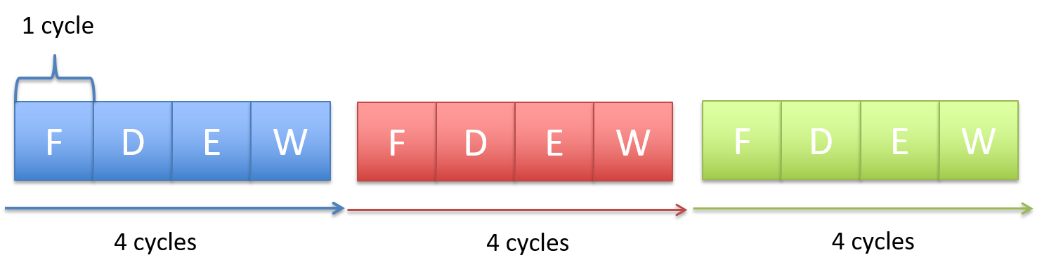
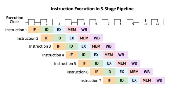
Instruction pipelining is the idea of starting the execution of the next instruction before the current instruction has fully completed its execution. That is, pipelining will execute instructions in order, but it allows the execution of a sequence of instructions to overlap.
For example, in the first cycle, the first instruction enters the Fetch stage. In the second cycle, that instruction advances to Decode while the second instruction begins Fetch. In the third cycle, the first instruction reaches Execute, the second moves to Decode, and the third begins Fetch. In the fourth cycle, the first instruction enters the Memory stage, and the fourth instruction begins in the Fetch stage.
Finally, the first instruction enters in the write-back stage, and completes, where the second advances to the Memory stage, the third to Execute, and the fourth to Decode. At this point (i.e. after the fifth cycle), the pipeline is fully loaded, and so each stage of the CPU is busy with a different instruction, each one step behind the previous (which forms the staircase in the figure below). Once the pipeline is full, the CPU can complete one instruction every clock cycle, greatly improving instruction throughput. On the other hand, if each fetch-decode-execute cycle is performed sequentially, the instruction throughput would remain constant.
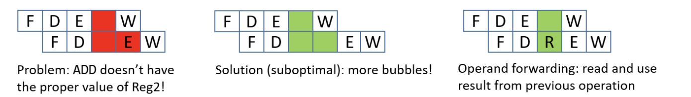
While pipelining improves instruction throughput by overlapping instruction stages, it can still suffer from hazards: a situation that prevents the next instruction in the pipeline from executing in its designated clock cycle. This causes the pipeline to stop or delay instruction advancement, which we call a pipeline stall. There are three particular hazards: data hazards, control hazards, and structural hazards. A data hazard is a hazard caused when an instruction depends on the result of a previous one that has not yet completed. A common solution involves inserting no operations (NOPs) (also called a pipeline bubbles) into the pipeline, notably the shorter instruction.
Consider the following instruction stream:
mov rax, qword ptr [0x84]   ; Load memory at 0x84 into RAX
add rax, 2                  ; Add 2 to RAX
The mov instruction (mov rax, qword ptr [0x84]) needs to read from memory (MEM stage) and then write the result to rax (WB stage), which takes five pipeline stages. The add instruction (add rax, 2) only needs four stages since it doesn't go through the MEM stage. Because pipelining overlaps these stages, both instructions can be "in flight" at once; parts of both are being executed simultaneously.
However, since the mov instruction hasn't finished writing to rax yet (it hasn't reached its WB stage), the add instruction, which depends on the updated value in rax, reaches its EX stage early and tries to read rax before mov's write-back is complete. This creates a read-after-write (RAW) hazard.
Also, since the mov takes five stages and the add takes four, their write-back stages line up so that both try to write to rax in the same cycle. This introduces another data hazard, a write-after-write (WAW) hazard.
To prevent this, the CPU can make all instructions effectively take five stages by inserting no operations (NOPs, or informally, pipeline bubbles).
NOPs delay the add until the mov has fully completed, preventing overlapping writes. However, inserting bubbles slows down the pipeline, since extra cycles are wasted waiting for results.

A more efficient solution is operand forwarding. Instead of stalling with NOPs, the CPU can forward the result of the mov instruction directly from the pipeline stage where it becomes available to the stage where the add needs it. This allows the add rax, 2 instruction to execute immediately once the loaded value is ready, without waiting for the mov to finish its write-back.
By using operand forwarding, the processor eliminates unnecessary bubbles, keeps the pipeline full, and executes both instructions efficiently.
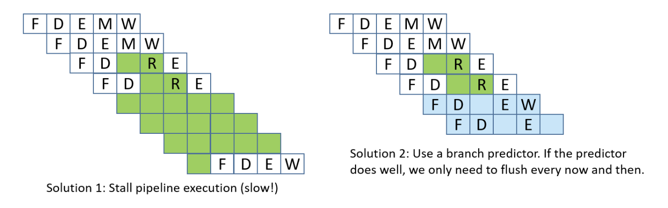
A control hazard is a hazard when the pipeline doesn't know which instruction to fetch next because it's waiting for the outcome of a conditional branch instruction. This can cause the pipeline to make a wrong guess, requiring it to flush the incorrectly fetched instructions and restart, which slows down performance. To address control hazards, many NOPs can be inserted by the compiler or assembler until the processor is sure that the branch is taken. Another solution involves eager execution, which execute both sides of the branch at the same time, and when the condition is finally known, it just chooses the right result. In x86, we see this through cmov. However, it brings some safety downsides, such as if one branch does something with side effects (like writing to memory or calling a function), you can't execute it speculatively without changing program behaviour, or if one branch dereferences a pointer that might be invalid, executing it early could cause a crash, and of course, inefficiency, as it also wastes work when one path's results are thrown away. The most interesting solution is branch prediction, which involves a branch predictor, that predicts which way a branch will go, based on previous executions.
Lastly, structural hazards are hazards that arise when two instructions need the same hardware resource at the same time.
Technique 2: Out-of-Order Execution
The CPU can be further optimized by allowing out-of-order execution. This means instructions that are independent of one another can be executed in a different order than they appear in the program, as long as the final results respect program order.
For example, consider this instruction stream:
r3 = r1 * r2r4 = r2 + r3r7 = r5 * r6r8 = r1 + r7
There are two data hazards: instruction 2 depends on the result of instruction 1 (it needs the value of r3), and instruction 4 depends on the result of instruction 3 (it needs the value of r7). However, instructions 2 and 3 are independent of each other. Instead of stalling the pipeline while waiting for instruction 1 to finish, the CPU can begin executing instruction 3 in parallel, ensuring that hardware units stay busy.
Technique 3: Superscalar Execution
Superscalar execution is an Instruction-Level Parallelism (ILP) technique where a processor issues and executes multiple independent instructions in a single clock cycle by using multiple execution units. A superscalar processor can achieve an IPC (instructions per cycle) greater than 1, unlike a scalar processor which executes at most one instruction per clock cycle. The processor's dispatch logic identifies independent instructions and simultaneously sends them to different execution units (e.g., multiple ALUs, FPUs, or load/store units).
Hardware Multithreading
The Problem: A single CPU core often sits idle waiting for things like:
- Memory to load data (very slow compared to CPU speed)
- Cache misses
- Branch mispredictions
- Other pipeline stalls
During these waits, the CPU is doing nothing, thereby wasting cycles.
The Solution (Hardware Multithreading): In a single core, have 2 independent copies of all the architectural state to maintain and execute multiple independent instruction streams (i.e., the sequence of instructions being executed). We call these duplicated architectural states hardware threads, or logical cores. When one instruction stream stalls waiting for memory, the CPU instantly switches to executing the other instruction stream instead of sitting idle.
Each hardware thread has:
- a complete set of general-purpose registers (e.g., 2 sets of RAX, RBX, RCX, etc. on x86)
- a program counter (each tracking a different position in code)
- a set of other architectural state (stack pointers, status flags, etc.)
And they share:
- The execution units (ALU, FPU, etc.)
- The caches (usually)
- The pipeline stages
Types of hardware multithreading
Interleaved Multithreading
- Based on scalar processors
- Shares a single pipeline and single ALU
- Executes instructions from only one hardware thread per cycle
- Switches between threads cycle-by-cycle or on stalls
- Cannot achieve IPC > 1
- Fine-grained interleaving (such as barrel processors) switches between threads every cycle, issuing instructions from different threads in rapid succession.
- Coarse-grained interleaving only switches threads when the currently running thread encounters a high-latency event (like a page fault). This approach is more common because it requires fewer context switches.
Simultaneous Multithreading (SMT)
- Based on superscalar processors
- Shares multiple pipelines and multiple execution units
- Can execute instructions from MULTIPLE hardware threads in the same cycle
- Can achieve IPC > 1
The term SMT is sometimes used loosely to refer to any hardware multithreading, but technically it only applies to simultaneous execution architectures.